Probing voltages
All voltage measurements in real circuits are actually measurements of voltage differences. In many cases such as when probing a voltage using an oscilloscope probe, it is easy to forget that the voltage being measured is, in reality, the difference between the voltage at the probe tip and wherever the probe ground lead is connected. In the same way it is easy to forget that probing a single ended voltage in a simulation schematic is with respect to wherever the ground node has been placed.
A common mistake, however, is to attach a voltage probe to ground.
In a real circuit, probing a voltage between any two points places a resistive load between them. With a good quality voltmeter that resistance may be very high, in the order of hundreds of MegΩ. With a x10 oscilloscope probe it will be 10MegΩ. There will be some stray capacitance across that resistance. There will also be stray lead inductances. If the voltage being measured is an AC signal then impedances due to these stray and parasitic components will also load the circuit.
Note that in simulations, voltage probes present an infinite resistance and have no stray capacitance or inductance. In effect, voltage probes have an infinite bandwidth.
The following example illustrates some of the probing techniques described above:
The following example shows a number of ways to measure voltages with respect to ground or differentially using;
-
The with a Voltage probe to probe the output;
-
An source (a.k.a. Voltage Controlled Voltage Source or VCVS) with a Voltage probe to probe the output;
-
A , source (a.k.a. behavioural or dependent source) configured as a VCVS using a Voltage probe to probe the output.
The schematic also demonstrates the importance of:
-
Giving voltage probes names that are identical to the nets to which they are attached;
-
Naming all nets in a schematic;
Connect Pad to Pad
When creating a PCB without a Schematic, none of the pads on the Footprints have nets connecting them so there will be no ratlines.
Rather than try to track the pads from scratch, it is a good idea to connect them up by hand first using from the PCB Tools palette. This will help you to remember to track the pads correctly with fewer mistakes.
You could also do this by setting net names for all the pads: if the two pads are given the same net name then EasyEDA will understand that they are connected together and will automatically create a ratline between them.
Or you can set these two pads with the same net name at the right panel Pad Properties after you click the pad.
Library
EasyEDA provide a lot of libraries, you can find them at “Left-hand Panel — Library”, hotkey “SHIFT+F”, at here you can search library from LCSC, system, user contributed etc.
Type
- Symbol: Schematic symbols
- Spice Symbol: Symbols for spice simlation
- Footprint: PCB footprints, PCB pattern.
- SCH Modules: Schematic modules, a part of the circuit design. It can not assign the PCB module, doesn’t like the schematic Symbol can assign the footprint . when it be placed on the schematic, it will be separated.
- PCB Modules: As like as Schematic modules.
- 3D Model: It is bind with footprint via “3D Model Manager”.
Classes
- Work Space: It include your personal parts and your teams’ parts.
- LCSC: EasyEDA online part store LCSC.com parts(Officail Parts). It will add new libraries everyday
- LCSC Assembled: JLCPCB Assembled parts. All JLCPCB assembly parts will contain a SMT icon, that means this part can be JLCPCB assemble.
- System: EasyEDA system parts, it comes from open source libraries, such as Kicad libraries, company public libraries, user contributions.
- Follow: If you follow a user at EasyEDA(You can follow a user at him/her user page), you can view and use his/her libraries.
- User Contributed: When you searching a part, maybe you can find it at this class. At EasyEDA, all libraries are public. the detail you can refer at: Contribute
We add an “JLCPCB Assembled” Components option of the Parts, It’s easy to choose which component can be assembled by JLCPCB. Yes, JLCPCB will provide the assembly service. the more information please refer at: How to order a SMT order
Search Engine — EasyEDA
Simply type your part number or symbol’s name to Search. before searching, you must choose the “Type” first.
and then click the “Table of contents” to open the categories list to choose your components.
From there you can scroll up and down to browse parts from each category.
If you know the component’s nameSuppose you want to find the MAX232 (which converts signals from an RS-232 serial port to signals suitable for use in TTL compatible digital logic circuits). Simply type Max232 into the Search box and press Enter:
- If you don’t know the component’s nameFor example, you want to find a resistor which value is 1kohm, footprint is 0603, at Libraries you can follow below steps:
- 1.Choose the library type
- 2.Typing the keyword such as
- 3.Click the search button
- 4.Select the class you which is wanted of the result
- 5.If you don’t need the search you need to remove all the search keywords
Search Engine — LCSC Electronics
When you want to find some parts by clearly parameter, you should try “Search Engine — LCSC Electronics”, it all most same as LCSC.com.
When you find out part, and you can place into the schematic:
Notice:
The subpart can not be preview at Preview dialog window, if you find out this, you need to change to “Search Engine — EasyEDA” to place this part.
Max and Min mode
If you want to place without close the “Library” dialog, you can change dialog mode to Min mode, just click the Min button at the top-right corner.
Operations
When you hover the mouse over the picture of the Schematic symbol or PCB footprint, you will find a toolbar with “Edit”, “Place”, “More” buttons.
Place:
For parts you use infrequently, you don’t need to Favorite them; just Place it into your canvas directly. Or you can double click the library to place.
Note:
-
EasyEDA supports multi-documents so please make sure that you are placing the part into the right (active) document. The active document is the one with the highlighted tab.
-
You can’t place a Schematic symbol into a PCB file, or a PCB Footprint into a schematic.
-
EasyEDA will try the best to make sure the library is correct, but it still has incorrect parts, if you find any incorrect parts please let us known. suggested order a sample first before ordering a big order.
Edit:
If you want to create your own version of a symbol or footprint then you can open an existing part from the library to use as a template, edit it and then save it to your local Work Space library in Library of the Navigation Panel.
More:
We can’t promise that every component in the library is free of errors so please check all symbols and footprints carefully before you commit to a PCB order.
If you do find a mistake in a component, please use the , so that we can fix it.
Components with sub parts (multi-device footprints).
When you find a component with sub-parts, you can’t Place or Edit it, but you can Favorite and Clone it as your own part, which you can then edit.
Right-Click
When you right-click the part list, you can edit its tags, add favorite etc.
Preview Image
Every library when you click, you can check its preview image, such as symbol, footprint, production picture. Click the the image you can open it quickly.
Предоставление доступа к проекту в EasyEDA
По умолчанию все ваши проекты будут приватными (напоминаю, что в EasyEDA, в отличии от других, не существует ограничения на количество приватных проектов). Для совместной работы над проектом вы можете предоставить доступ своему коллеге (коллегам). Вы можете предоставить доступ только для чтения (read-only) или полный (read/write) конкретному пользователю, для этого нужно кликнуть правой кнопкой мыши по названию проекта и ввести адрес электронной почты, на который зарегистрирован аккаунт EasyEDA вашего коллеги.
Предоставление доступа к проекту EasyEDA
Предоставление доступа к проекту конкретному пользователю в EasyEDA
6: PartSim
PartSim выделяет возможность трудиться с простыми схемами и с теми, у которых изменены свойства каких-либо составляющих, частотных и количественных данных источников сигнала и рабочего тока. Понятный интерфейс позволяет быстро разобраться, как производятся главные операции, изменять рабочий макет, вставлять или удалять графические составляющие.
Способности PartSim не слишком отличаются от других аналогичных систем. Здесь можно создавать и сохранять проекты, распечатывать результаты, менять характеристики составляющих (сопротивлений, емкостей, различных видов источников токов и генераторов входных сигналов). Кроме этого, утилита предлагает расчет и графическое изображение процессов, которые протекают в создаваемой электросхеме в реальности (функция осциллографа).
Возможно подтверждение подлинности данных электронной схемы. Для этого полученное графическое изображение сопоставляется с расчетными значениями, которые отображаются на листинге проекта (Current Netlist). Рабочая среда предлагает такие функции:
- создание с нуля на отдельном листе новой схемы;
- продолжение уже существующего проекта;
- организация разработки отдельного этапа многостраничной схемы, которую позже можно подключить к базовому варианту.
С PartSim нетрудно видоизменить рабочую схему, внести в базу новые составляющие, высчитать ключевые характеристики и получать графики, где указаны значения частоты и амплитуды. Среда моделирования всегда выдает правильные результаты анализа по DC, DC Sweep, AC и переходным процессам, что позволяет применять ее и для изучения основ проектирования электронных устройств, проведения проверки схем, созданных на элементной базе от Digi-Key.
Интерфейс программы представлен только на английском языке.
Добавление компонентов в схему EasyEDA
Подключим к ESP8266 светодиод. В качестве шпаргалки воспользуемся замечательным наглядным пособием Arduino Basic Connections — подключение всего в картинках v 2.0 Если вы новичок и еще не видели этот документ, то рекомендую сделать его вашей настольной книгой, чтобы избежать множества граблей, которые подстерегают начинающих радиолюбителей. Также хочу вам сообщить, что и ESP8266 и ATMEGA на Arduino являются микроконтроллерами и принципы подключения к ним периферии одни и те же, поэтому вы можете смело использовать рекомендации по Arduino для ESP8266, при этом не забывайте о том, что:
- Arduino бывают как 5-ти вольтовые, так и 3.3, а ESP8266 только 3,3
- Порты Arduino выдерживают ток до 40мА, а ESP8266 — только 12мА
Подключение светодиода к выходу микроконтроллера
Возьмем из шпаргалки левый вариант, где мы видим, что для подключения светодиода нам нужен резистор и питание. При низком уровне на выходе GPIO светодиод будет включаться, а при высоком выключаться.
Скопируем элемент VCC из левой части схемы: левый клик мышью на элементе (не промахнитесь — вам нужна и надпись VCC и «частичка провода»), затем Копировать на панели инструментов и там же Вставить — эта процедура абсолютно аналогична действиям в обычном текстовом редакторе. Вставляемый элемент «прилипнет» к указателю мыши и вы вставляете его в правую часть схемы в свободное место кликом мыши.
Копирование и вставка в EasyEDA
Добавим резистор из Библиотеки EasyEDA
Выбираем привычный нам «европейский» символ компонента в EasyEDA
Pad
You can add pads using the Pads button from the Footprint Tools palette or using the hotkey.
After selecting one of the pads, you can view and adjust its attributes in the right hand Properties panel.
Number: Remembering the pin numbers you set in the schematic symbol in your Schematic Lib: to connect those schematic symbol pins to the pads in your PCB footprint, the pad numbers you set here in the Footprint footprint must be the same.
Shape: Round , Rectangular , Oval and Polygon.
EasyEDA supports four shapes: , , and .
- PAD will give your more space.
- PAD will let you to create some strange pad.
Like in the image below, you can edit the PADs points when you select a PAD
Layer: If the pads are part of a SMD footprint, you can set it to Top layer or Bottom layer. For through hole components you should set it to Multi-Layer. If it setting as mult-layer, it will connect with all copper layers.
Net: You don’t need to enter anything here because at present this footprint is not connected to anything in a circuit.
Width and Height: When the shape is set to Round, Width will equal Height.
Rotation: Here you can set the Pad’s rotation as you want.
Hole(D): This is the drill hole diameter for a through hole pad. For a SMD Pad, set its layer to TopLayer or BottomLayer.
Hole Shape: Round and Slot. When it is set as a slot, the Gerber is generated through the stitching of multiple drill holes in the corresponding position. If your hole is round, please do not set it as a slot, so as to avoid the overlapping error of holes during the production of DFM detection.
Center-X and Center-Y: using these two attributes, you can set the pad’s position with more precision, compared to using the mouse.
Plated: Yes or No. When you set it as No, this pad Inner wall do not metallization.
Paste Mask Expansion: For single layer pad. This property affects the size of the tin area on the plate of the steel mesh. If you want to set a pad that is not open in the steel mesh, you can set the value to be negative, which is usually larger than the diagonal of the pad.
Solder Mask Expansion: This property affects the size of the green oil area cover on the pad. If you want to set a pad not open covered with green oil, you can set the value to be negative, the value is usually set larger than the diagonal of the pad.
And you can select a track/Solid Region, right-click it and convert to a pad.
Image
On PCB and Footprint editor, there is a nice feature on the PCB Tools bar.
After clicking on the image icon, you will see the Insert Image window as below.
In this dialog, you can choose your favorite image, EasyEDA support , , , , and . Unlike some other EDA tools which only support a Monochrome Bitmap image, EasyEDA supports full color, but Monochrome Bitmap is welcome.
You can adjust the color tolerance, simplify level and reset the image size there.
And you can select shape invert.
The image will be inserted to the active layer, if it is not right, you can change the attribute. Such as TopSilkLayer.
Создание нового проекта в EasyEDA
Проект в EasyEDA — это совокупность схем и данных о разметке вашей платы. Так что если вы планируете даже просто нарисовать схему, то вы должны создать новый проект и уже в нем создать новую схему. Это может показаться лишним действием, однако приучит вас к порядку раскладывать все по папочкам. У вас же не лежат все документы на рабочем столе без папок? Или все таки да 🙂
Новый проект можно создать «с нуля» или склонировать у кого-то уже существующий (как это сделать будет показано ниже). Также кто-то может предоставить вам доступ к своему проекту для совместной работы.
Создание вашего первого проекта в EasyEDA
Создание нового проекта в EasyEDA
Далее вам предлагается ввести название проекта и указать: будет ли ваш проект публичным (проект будет доступе в поиске и кто угодно сможет его склонировать себе в редактор и производить над копией любые действия), либо ваш проект будет приватным и посторонние не получат к нему доступа до тех пор, пока вы этого не захотите. Публичность/приватность проекта можно менять в последующем неограниченное количество раз.
Задайте подробное описание вашего проекта в поле Description.
Выберите тип вашего проекта: приватный или публичный
Возможности EasyEDA
- Редактор схем
- Удобный интерфейс с кучей библиотек. Умеет импортировать файлы из LTSpice, Altium Designer и Eagle
- Редактор печатных плат
- Позволяет развести печатную плату из схемы. Возможность экспорта в gerber. Имеет неплохой автороутер
- Spice-симулятор
- Умеет работать с цифровыми, аналоговыми и смешанными сигналами, облачные сервисы обеспечивают быстрое моделирование
- Редактор блок-схем
- Может, кому-нибудь пригодится
- Горячие клавиши
- Множество операций удобно выполнять горячими клавишами, которые можно настроить — всего 64 комбинации
- Экспорт
- Печатные платы — Protel, Kicad, PADS
рисунки — PDF, SVG, PNG
умеет экспортировать схемы и платы в JSON-формат - Импорт
- Altium/ProtelDXP Ascii Schematic/PCB
Eagle схемы, печатные платы и библиотеки
библиотеки и модули Kicad
Spice — модели
Окно редактора схем выглядит следующим образом:
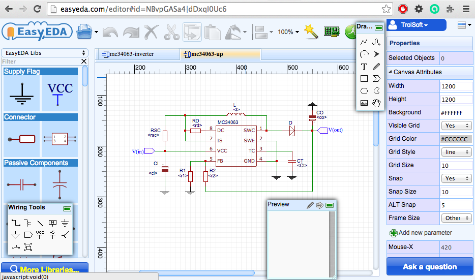
Центральная область экрана отображает схему или печатную плату. Причем, одновременно можно держать открытыми множество схем/плат — такой возможности
нет даже в Eagle! На панели слева можно выбирать компоненты из библиотеки EasyEDA или своих собственных. Чтобы перенести компонент на схему, надо
кликнуть по нему и курсор мыши примет вид этого компонента. Затем, если кликнуть по схеме, компонент будет помещен в место клика. Также, в левой
панели можно осуществлять навигацию между своими проектами.
Чтобы соединять элементы между собой, есть плавающее окно «Wiring Tools». Окно «Drawing Tools» позволяет добавлять пояснительные надписи, фигуры
и рисунки. А кликнув по элементу можно редактировать его свойства в правой панели.
Этот интересный проект доступен по адресу
http://easyeda.com
После некоторого опыта использования продукта можно сказать, что он вполне юзабелен, хоть и всё ещё сыроват. До тех пор, пока у Eagle CAD были
ограничения на размер платы, имело смысл осваивать EasyEDA привыкая к его особенностям и некритичным багам. Но, после того, как Eagle был
куплен Autodesk-ом и ограничение на максимальный размер платы в бесплатной версии было снято, EasyEDA, как мне кажется, ощутимо утратил свою актуальность.
Create the Schematic Symbol
Using Schematic Symbol Wizard and Group/Ungroup… is a quick way to create schematic symbols but they are placed directly into the schematic that they are built in.
It is possible to reuse them by copying them ( hotkeys) from the schematic they were created in and then cross-document-pasting them ( hotkeys) into a different schematic but this quickly gets messy if you need to copy symbols that were created in several different schematics.
OK, you could keep copying new symbols into a dedicated “symbol library” schematic sheet to save searching for them but EasyEDA offers you an easier way to create and manage your symbols in a library.
Start a new Schematic Lib as shown below or by doing:
1. File > New > SymbolThis opens the New SchematicLib symbol editor.
2. Create the symbol
-
Get the DatasheetFor example, using the NE555DR, the datasheet you can refer LCSC: NE555DR.And then create the symbol and place the pins for the library base on the datasheet.This component have 8 pins and names.
-
Create via Schematic Symbol WizardThe more information of Schematic Symbol Wizard please refer next section.
-
Create by Manually
-
Draw the shape via the Drawing Tools
-
Place the PinsThe Pin dot must keep out side as the image indicated, it is connecting with the wires. The more information please refer SchematicLib Attributes — Pins Section.
-
3. Edit the pin mapVia Edit > Pin Map…, change Pin names and Pin numbers. For some complicated IC, will use the alphabet for the pin number.
4. Modify the Detailsuch as change Pin length, place text, change Pin color, Pin attributes etc.
5. Set Costom AttributesYou can set the supplier, footprint(Suggested, you must assign the footprint via “Footprint Manager”), Name(Required), Prefix(Required) for it, the more detail of attributes please refer below section: Custom Attributes
If the schematiclib need to assign the packahe, the Pin number should match the footprint’s Pad number. The detail of the footprint assign please refer the Footprint Manager section at previous.
If the part’s property “Convert to PCB” is set as “No”, it will not appear at footprint manager.
6. Set the OriginYou can via: “Top Menu — Place — Set Canvas Origin — By Center Grid of Symbols” to set the origin.
7. Save your SchameticLibYou can set this library’s owner, datasheet link and tags etc.
Then a Schematic Symbol is created finish. And the you can find it at “Libraries — SchematicLib — Personl” on the left-hand.
Notice:
- Note the Origin Point. To simplify rotating your symbols when they are placed into the canvas, make sure all of your symbols are created as near as possible centered around that point. Suggesting the first Pin/Pad or its center to be the origin point.
- Please make sure all pins dot are placed on the grid, otherwise, when place the library on the schematic will causing the wiring difficult.
Connect Pad to Pad
When creating a PCB without a Schematic, none of the pads on the Footprints have nets connecting them so there will be no ratlines.
Rather than try to track the pads from scratch, it is a good idea to connect them up by hand first using from the PCB Tools palette. This will help you to remember to track the pads correctly with fewer mistakes.
You could also do this by setting net names for all the pads: if the two pads are given the same net name then EasyEDA will understand that they are connected together and will automatically create a ratline between them.
Or you can set these two pads with the same net name at the right panel Pad Properties after you click the pad.
Создание новой схемы в проекте EasyEDA
Создадим новую схему в нашем проекте — это можно сделать «с нуля» (ссылка справа на скриншоте), из шаблона (ссылка слева) или из внешнего файла (ищите импорт в меню). Тут вас ожидает приятный сюрприз: в системе уже есть шаблон схемы с минимальной обвязкой для модуля ESP8266 (ссылка слева на скриншоте). Вы можете создавать собственные шаблоны для последующего быстрого старта проектирования однотипных схем, что может оказаться весьма полезным.
Создание новой схемы в EasyEDA
При создании новой схемы по правой ссылке, вы создаете схему не совсем «с нуля», как я вам сообщил выше. Вам будет предложено нарисовать новую схему в рамке, по буржуйским стандартам
Новая схема в буржуйской рамке в EasyEDA
Возможность сделать рамку по ГОСТу, я думаю тоже есть, если самому нарисовать для нее собственный шаблон и начинать каждую новую схему уже с него. Может быть это уже кто-то и сделал, а вам осталось лишь «форкнуть» этот проект.
Схемы и библиотеки в проект можно импортировать из файлов на вашем компьютере, поддерживаются популярные форматы:
Импортирование схем и библиотек в EasyEDA
Мы, для примера, создадим новую схему из шаблона для ESP8266.
CIRCUIT LAB
Circuit Lab – это многофункциональный онлайн-симулятор схем, но он не бесплатный. Он разработан с простым в использовании редактором и точным аналоговым / цифровым схемным симулятором.
Преимущества Circuit Lab:
- Эта платформа хорошо выполнена и имеет довольно обширную библиотеку, которая подходит как для начинающих, так и для опытных экспериментаторов
- Смоделированные графики и выходные результаты можно экспортировать в виде файла CSV для дальнейшего анализа
- Проектирование цепей выполняется легко, и доступны предварительно разработанные схемы
Недостатки Circuit Lab:
- Это не бесплатная платформа, но вы можете использовать демонстрационную версию бесплатно
- Моделирование могло бы быть лучше с интерактивными симуляциями кроме графического представления
- Больше цифровых микросхем следовало бы добавить в библиотеку
Probing currents
In a real circuit, probing the current in a wire places a resistive load between them. This will cause some voltage drop across the ammeter. With a good quality ammeter that voltage drop may be very low, in the order of millivolts. There will be some stray capacitance across the insertion resistance and from the ammeter connections to ground. There will also be stray lead inductances. If the current being measured is an AC signal then impedances due to these stray and parasitic components will also load the circuit.
Note that in simulations, except for the Ammeter, which has a 1uΩ (1e-6Ω) series resistance, current probes present zero insertion resistance and have no stray capacitance or inductance. In effect, current probes have an infinite bandwidth.
The following example shows a number of ways to measure currents with respect to ground or differentially using;
- As a current using the Ammeter symbol;
- As a linearly scaled voltage using an H Current Controlled Voltage Source (CCVS) (or an F Current Controlled Current Source (CCCS) with a resistor);
- As a linearly scaled current using an F Current Controlled Current Source (CCCS) driving an Ammeter;
- As a voltage that can be an arbitrary function of the current flowing through a 0V Voltage Source using a BV source (or a BI source with a resistor);
- As a current that can be an arbitrary function of the current flowing through a 0V Voltage Source using a BI source driving an Ammeter.
Note however, that although a 0V source can be used to monitor a current, it cannot be used to measure a current so that it can be directly displayed in the Simulation > Show your simulation report… window or plotted in Waveform.
Pin Attributes
Symbols pins are the most important part of any Schematic Lib symbol. They are the things that allow wires to be attached to symbols to connect up your circuit.
You can use the P hotkey to add a Pin or from the Draw Tools pallete:
Before placing it on the canvas, you can use the rotation hotkey or rotate and flip from the menu to rotate it to the right orientation. Make sure the Pin Dot(black dot) is in the right position. The Pin Dot will be used to connect your wires or netlabels. Whenever a PIN is either placed as directly onto the canvas or as part of a symbol, the mouse has to point to the Pin Dot position to automatically start the Wire mode or to join a wire to it.
Whenever a Pin is placed as part of a symbol, the Pin dot should be outside of — and pointing away from — the symbol like in example 1(correct position), inside or pointing towards the symbol as shown in example 2(wrong position).
When you select a single Pin, the Pin attributes will be shown in the right hand Properties panel:
Orientation: 0°,90°, 180° and 270°。If you want to create a 45° pin, you need to set it length as 0, and draw a line with 45°。
Start-X and Start-Y: The pindot position. Sometimes it may be difficult to move the pin to the desired position using the mouse, so you can move the pin via Start-X and Start-Y.
Length: Pin length.
Name: In this example, VCC is the name of the Pin.
Number: In this example, 1 is the number of the Pin. This number is the pin number of the device in a physical footprint.
Note that you can use alphanumeric identifiers such as; A1, B1, C1, A2, B2 and so on as the Number.
Spice Number: These are the pin numbers used to connect your symbol to the corresponding pins defined by the .model or .subckt used to simulate your device. The pin numbers of the simulation model may be different from the physical footprint pin numbers and — unless the model is specifically created to model multiple devices in a single footprint — do not change for different instances of a device in a multi-device footprint. The Spice Pin order must be numerals only.
Name Display: If you don’t want to show VCC, switch it to NO.
Number Display: If you don’t want to show 1, switch it to NO.
You can adjust the Name or Number position using your mouse but note that rotate and flip applies to the whole pin including the name and pin number; these items cannot be rotated and flipped independently of the pin itself.
Note also that rotate and flip actions do not result in upside down or mirrored pin number or names.
Color: You can set the Pin to different colours, such as PIN3:CLK as orange and PIN4:GND as blue. In this example, the PIN1 is set as color , but it shows as red, because it is selected. After deselecting it, the pin will appear color .
Dot: adds a circle to the inside end of the pin to indicate logical (or analogue) inversion.
Clk: adds a to the inside end of the pin to indicate that the pin is logical clock input.
Show: YES/NO. Allows you to hide the pin. When set it to NO, this Pin will be hidden when the symbol is placed on the schematic editor canvas, and then create a net which name same as this pin name.
Note that the pin is not hidden here in the Schematic Lib symbol editor canvas because if it was, it would disappear from view and so how would you find it to make it visible again? For the same reason this option has no effect in symbols made using Group/Ungroup…
We may not have thought of everything in EasyEDA but we do try. 🙂
Electric: [Undefined, Input, Output, I/O, Power]
EasyEDA provides Electrical Rules Checking (ERC) right now, But you still need to set electric of your Schematic libs.
If you set the PIN as Power and set the pin to be hidden, then the Pin will be connected by Name which is the NetLabel. If the Name is VCC, it will be connected to the net in your circuit with the NetLabel or NetFlag VCC. This is helps to keep the schematic clear and uncluttered when using Multi-part Components.
After created the Lib, use will open the save dialog:
After clicking Save, you will see it appears in Libraries > Symbols > Personal of the left hand Navigation panel.
If you want to modify the tag for your new symbol: Libraries > Symbols > Personal > Select New Lib > More > Modify, or right-click new Lib > Modify, if your Lib doesn’t have the tags it will appears on All.
7: 123DCircuits
123D Circuits включает в себя целый перечень полезных возможностей для создания электросхем. После единоразовой регистрации на сайте (при последующих входах нужно будет вносить данные учетной записи) пользователь может выбирать между разными опциями: создание нового проекта, добавление элементов или импорт цепей из программы Eagle. Размеры плат тоже предоставляются на выбор, кроме того, поддерживается свободное размещение текста и метод шелкографии.
Основная особенность 123D Circuits – это копирование платформы Arduino, поддержка плат ввода/вывода и возможность корректировки кода программы из браузера в видимом режиме.
Моделируются электросхемы в редакторе при помощи набрасывания проводов и нужных элементов на макетную плату, после этого они подключаются к виртуальному процессору. Кроме того, в программе всегда можно проводить диагностику, анализ и интерактивную имитацию работы цепи в реальности.
Библиотека элементов сейчас совсем небольшая, доступны образцы только главных элементов: электронный элемент с 2 электродами, светоизлучающий диод, двухполюсник с малой проводимостью, индуктивность, сопротивление, транзистор, кнопка, потенциометр, DC-мотор, мультиметр и некоторые другие. При этом мощный и одновременно простой редактор позволяет добавлять новые радиокомпоненты, которые требуются в проекте.
Работа с виртуальной средой начинается сразу после внесения необходимых личных данных на сайте. В разделе Help можно найти ответы на все вопросы, которые касаются работы с этим продуктом. Бесплатная версия системы предлагает большое количество схем (т. е. доступных любому пользователю).
Веб-приложение не предъявляет особых требований к гаджетам пользователей. Достаточно бесперебойного соединения с интернетом на высокой скорости. Несмотря на то что программа 123D Circuits рекомендована для создания электрических цепей устройств среднего и высокого уровней сложности, некоторые этапы работы (в частности создание нового проекта, симуляция и анализ) занимают длительное время.