Реализация счетчика
Verilog Code:
- //——————————————————
- // Это моя вторая Конструкция в Verilog
- // Название Конструкции : first_counter (первый чсетчик)
- // Имя файла : first_counter.v
- // Функции : Это 4-х битовый суммирующий счетчик с
- // синхронным сбросом высокого уровня и
- // с разрешающим сигналом активного высокого уровня
- //——————————————————
- module first_counter (
- clock , // запуск входа счетчика
- reset , // синхронный сброс с активным высоким уровнем сигнала
- enable , // Разрешающий сигнал для счетчика с активным высоким уровнем
- counter_out // 4-х битовый вектор выхода счетчика
- ); Конец списка портов
- //————-Input Ports—————————— (порты ввода)
- input clock ;
- input reset ;
- input enable ;
- //————-Output Ports—————————-(порты ввода)
- output 3 counter_out ;
- //————-Input ports Data Type——————-(тип данных портов ввода)
- // По правилам — все порты ввода должны быть шинами
- wire clock ;
- wire reset ;
- wire enable ;
- //————-Output Ports Data Type——————(тип данных портов вывода)
- // Портами вывода могут быть ячейки памяти (reg) или шины
- reg 3 counter_out ;
- //————Отсюда начинается код ————————-
- // Поскольку это счетчик с запуском по положительному фронту,
- //В список чувствительности блока, записанного ниже, добавляем положительный
- // фронт сигнала clock.
- always @ (posedge clock)
- begin COUNTER // Имя блока
- // При каждом положительном фронте сигнала clock мы проверяем вход reset
- // Если на входе reset логическая единица, мы загружаем в выход счетчика нули (4’b0000)
- if (reset == 1’b1) begin
- counter_out <= #1 4’b0000;
- end
- // Если на входе reset ноль, мы увеличиваем содержание счетчика
- else if (enable == 1’b1) begin
- counter_out <= #1 counter_out + 1;
- end
- end // Конец блока счетчика
- end // Коней модуля счетчика
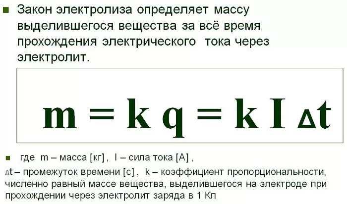
DC Simulation
For the DC simulation, we will sweep the input of the inverter, 0 to 5 volts.
To do this, first open up the schematic that is set up to simulate the inverter.
Then, select Tools -> Analog Environment, to open the Cadence Analog
Design Environment window.
Verify that the simulator that you are using is «spectreS». If not, change
the simulator to spectreS by selecting Setup -> Simulator/Directory/Host …
Now, select Analyses -> Choose …
Select the DC box under the analysis list. Also, select «Component Parameter»
and «Select Component». In the Virtuoso schematic window, select the voltage
source that is connected to the input of the inverter. A list of parameters of
the voltage source will appear. Choose «dc» and make sure in the analysis setup
window, that the Sweep Range has «Start-Stop» selected and 0 and 5 are in the
«Start» and «Stop» parameters, respectively. Also, make sure that the Sweep Type
reads «Automatic».
Now, you are ready to simulate. Select the output and input of the inverter
to plot and run the simulation. The DC Response should look something like the
waveform below.
Notice how the input and output cross in the linear (transition) region of
the inverter. We will want to calculate this crossing value so that it can be
used as a bias to the input of the inverter for future AC simulation. This can
be accomplished either by eyeing it or more effectively by using the calculator.
Open the calculator by selecting the calculator icon. Make sure that
«Evaluate Buffer» is unchecked. Select wave, and then click on the output
waveform in the Waveform Window. Now, select «Special Functions» and choose
«cross» in the Calculator window. When the «Threshold Crossing» window appears,
select OK for the default values. Select «Evaulate Buffer» in the Calculator
Window, and the cross value will be given. This should be roughly vdd/2 (vdd/2
is for an ideal inverter). Round off to the nearest hundreth and remember this
value for AC simulation.
Synchronizers for Clock Domain Crossing (CDC)
A synchronizer is a circuit whose purpose is to minimize the probability of a synchronization failure. We want the metastability to resolve within a synchronization period (a period of the destination clock) so that we can safely sample the output of the flip-flop in the destination clock domain. It is possible to calculate the failure rate of a synchronizer, and this is called the mean time between failure (MTBF).
Without going into the math, the takeaway is that the probability of hitting a metastable state in a clock domain crossing (CDC) is proportional to:
- Frequency of the destination domain
- Rate of data crossing the clock boundary
This result gives us some ideas on how to design a good synchronizer. Interested readers can refer to Metastability and Synchronizers: A Tutorial for a tutorial on the topic of metastability, and some interesting graphs of how flip-flops can become metastable.
Two flip-flop synchronizer
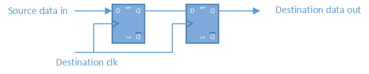
The most basic synchronizer is two flip-flop in series, both clocked by the destination clock. This simple and unassuming circuit is called a two flip-flop synchronizer. If the input data changes very close to the receiving clock edge (within setup/hold time), the first flip-flop in the synchronizer may go metastable, but there is still a full clock for the signal to become stable before being sampled by the second flip-flop. The destination domain logic then uses the output from the second flip-flop. Theoretically it is possible for the signal to still be metastable by the time it is clocked into the second flip-flop (every MTBF years). In that case a synchronization failure occurs and the design would likely malfunction.
The two flip-flop synchronizer is sufficient for many applications. Very high speed designs may require a three flip-flop synchronizer to give sufficient MTBF. To further increase MTBF, two flip-flop synchronizers are sometimes built from fast library cells (low threshold voltage) that have better setup/hold time characteristics.
Registering source signals into the synchronizer
It is a generally good practice to register signals in the source clock domain before sending them across the clock domain crossing (CDC) into synchronizers. This eliminates combinational glitches, which can effectively increase the rate of data crossing the clock boundary, reducing MTBF of the synchronizer.
10.2. Verilog, VHDL and SystemVerilog
Both Verilog and VHDL languages have their own advantages. Note that, the codes of this tutorial are implemented using VHDL in the other tutorial ‘FPGA designs with VHDL’ which is available on the website. If we compare the Verilog language with the VHDL language, we can observe the following things,
- Verilog has a very limited set of keywords; but we can implement all the VHDL designs using Verilog.
- Verilog codes are smaller as compare to VHDL codes.
- VHDL is strongly typed language, therefore lots of conversions may require in it, which make the codes more complex than the Verilog codes. Also due to this reason, it may take more time to write the VHDL codes than the Verilog codes.
- The general purpose ‘always’ block’ of Verilog needs to be used very carefully. It is the designer’s responsibility to use it correctly, as Verilog does not provide any option to check the rules. Any misuse of ‘always’ block will result in different ‘simulation’ and ‘synthesis’ results, which is very hard to debug. Whereas the behavior of VHDL is accurate, i.e. there is no ambiguity between the simulation and synthesize results.
- The user-defined type (enumerated type) can not be defined in Verilog, which is a very handy tool in VHDL for designing the FSM.
The SystemVerilog language is the superset of Verilog and contains various features of other programming language i.e. C (structure, and typedef), C++ (class and object) and VHDL (enumerated data type, continue and break statements). Most importantly, it replaces the general purpose ‘always’ block with three different blocks i.e. ‘always_ff’, ‘always_comb’ and ‘always_latch’, which remove the Verilog’s ambiguity between simulation and synthesis results. Also, the compiler can catch the error if these new always-blocks are not implemented according to predefined rules. In this chapter, we will reimplement the some of the designs of previous chapters using SystemVerilog to learn and compare the SystemVerilog with Verilog.
Assigning values to Verilog reg, Verilog wire
Verilog net data types can only be assigned values by continuous assignments. This means using constructs like continuous assignment statement (assign statement), or drive it from an output port. A continuous assignment drives a net similar to how a gate drives a net. The expression on the right hand side can be thought of as a combinatorial circuit that drives the net continuously.
Verilog variable data types can only be assigned values using procedural assignments. This means inside an always block, an initial block, a task, a function. The assignment occurs on some kind of trigger (like the posedge of a clock), after which the variable retains its value until the next assignment (at the next trigger). This makes variables ideal for modeling storage elements like flip-flops.
Verilog rule of thmb 2: drive a Verilog wire with assign statement or port output, and drive a Verilog reg from an always block. If you want to drive a physical connection with combinatorial logic inside an always@(*) block, then you have to declare the physical connection as Verilog reg.
1.1. Introduction
In this tutorial, full adder is designed with the help of half adders. Here we will learn following methods to create/implement the digital designs using Altera-Quartus software,
- Digital design using ‘block schematics’,
- Digital design using ‘Verilog codes’,
- Manual pin assignment for implementation,
- Pin assignments using ‘.csv’ file,
- Loading the design on FPGA.
- Converting the ‘Verilog design’ to ‘Symbols’
- Converting the ‘Block schematic’ to ‘Verilog code’ and ‘Symbols’.
If you do not have the FPGA-board, then skip the last part i.e. ‘loading the design on FPGA’. Simulation of the designs using ‘Modelsim’ is discussed in .
1.4. Manual pin assignment and compilation
Please enter correct pin location according to your FPGA board, as shown in this section. If you do not have the board, then skip this section and go to .
Once design is analyzed, then next step is to assign the correct pin location to input and output ports. This can be done manually or using .csv file. In this section, we will assign pin manually. Follow the below steps for pin assignments,
First open the ‘Pin-planner’ by clicking Assignments–>Pin Planner as shown in Fig. 1.12.
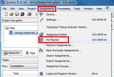
Fig. 1.12 Pin planner
Next, type the names of the input and output ports along with the pin-locations on the board, as shown in Fig. 1.13. Details of the Pin-locations are provided with the manual of the FPGA-boards e.g. in DE2-115 board, pin ‘PIN_AB28’ is connected with switch SW0. By assign this pin to ‘x’, we are connecting the port ‘x’ with switch SW0.
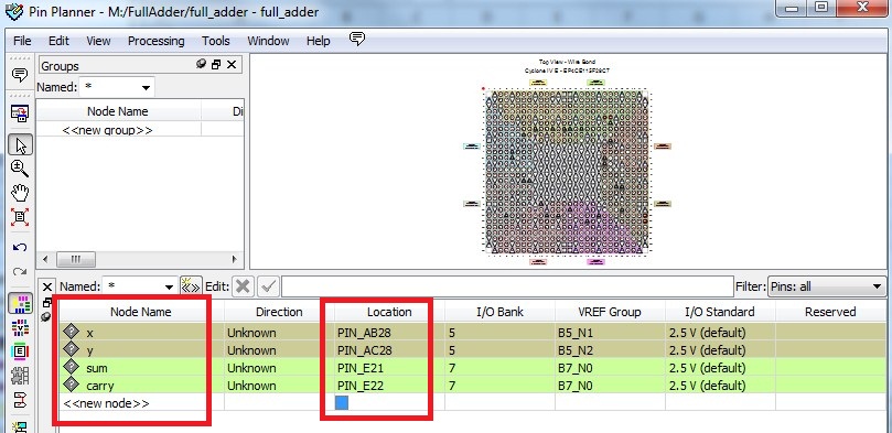
Fig. 1.13 Pin assignment
After assigning the pin, analyze the design again (see Fig. 1.11). After this, we can see the pin numbers in the ‘.bdf’ file, as shown in Fig. 1.14.
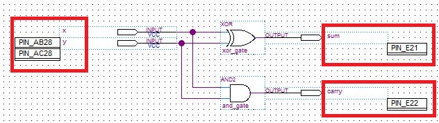
Fig. 1.14 Assigned pins to ports
Finally, compile the design using ‘ctrl+L’ button (or by clicking processing–>Start compilation, as shown in Fig. 1.15).
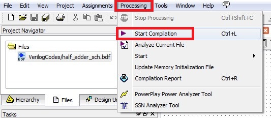
Fig. 1.15 Start compilation
After successful compilation, if we see the pin-assignment again, then we will find that direction of the pin are assigned now, as shown in Fig. 1.16 (which were set to ‘unknown’ during analysis as in Fig. 1.13)
7.4. Glitches
Glitches are the short duration pulses which are generated in the combinational circuits. These are generated when more than two inputs change their values simultaneously. Glitches can be categorized as ‘static glitches’ and ‘dynamic glitches’. Static glitches are further divided into two groups i.e. ‘static-0’ and ‘static-1’. ‘Static-0’ glitch is the glitch which occurs in logic ‘0’ signal i.e. one short pulse i.e. ‘high-pulse (logic-1)’ appears in logic-0 signal (and the signal settles down). Dynamic glitch is the glitch in which multiple short pulses appear before the signal settles down.
Note
Most of the times, the glitches are not the problem in the design. Glitches create problem when it occur in the outputs, which are used as clock for the other circuits. In this case, glitches will trigger the next circuits, which will result in incorrect outputs. In such cases, it is very important to remove these glitches. In this section, the glitches are shown for three cases. Since, clocks are used in synchronous designs, therefore Section is of our main interest.
7.4.1. Combinational design in asynchronous circuit
shows the truth-table for \(2 \times 1\) multiplexer and corresponding Karnaugh map is shown in . Note that, the glitches occurs in the circuit, when we exclude the ‘red part’ of the solution from the , which results in minimum-gate solution, but at the same time the solution is disjoint. To remove the glitch, we can add the prime-implicant in red-part as well. This solution is good, if there are few such gates are required; however if the number of inputs are very high, whose values are changing simultaneously then this solution is not practical, as we need to add large number of gates.
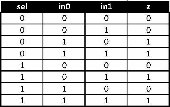
Fig. 7.4 Truth table of \(2 \times 1\) Multiplexer
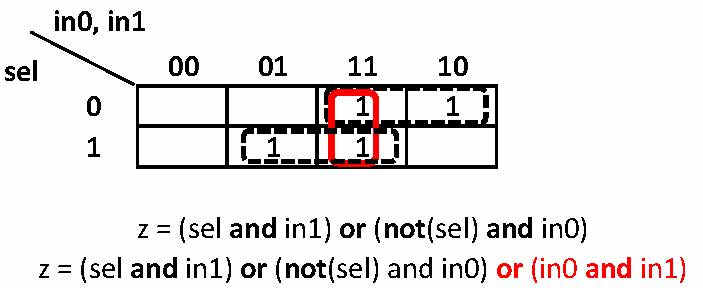
Fig. 7.5 Reason for glitches and solution
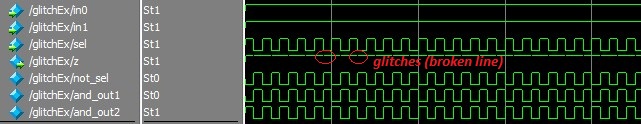
Fig. 7.6 Glitches (see disjoint lines in ‘z’) in design in
Listing 7.3 Glitches in multiplexer
1 2 3 4 5 6 7 8 9 10 11 12 13 14 15 16 17 18 19 20 |
// glitchEx.vhd

// 2x1 Multiplexer using logic-gates

module glitchEx(
    input wire in0, in1, sel,
    output wire z
);

wire not_sel;
wire and_out1, and_out2;

assign not_sel = ~sel;
assign and_out1 = not_sel & in0;
assign and_out2 = sel & in1;
assign z = and_out1 | and_out2; // glitch in signal z

//  // Comment above line and uncomment below line to remove glitches
//  z <= and_out1 or and_out2 or (in0 and in1);
endmodule
|
7.4.2. Unfixable Glitch
is another example of glitches in the design as shown in . Here, glitches are continuous i.e. these are occurring at every change in signal ‘din’. Such glitches are removed by using D-flip-flop as shown in Section . Since the output of Manchester code depends on both edges of clock (i.e. half of the output changes on +ve edge and other half changes at -ve edge), therefore such glitches are unfixable; as in Verilog both edges can not be connected to one D flip flop.
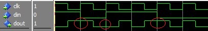
Fig. 7.7 Glitches in
Listing 7.4 Glitches in Manchester coding
1 2 3 4 5 6 7 8 9 10 11 12 |
// manchester_code.vhd

module manchester_code
(
    input wire clk, din,
    output wire dout
);

// glitch will occure on transition of signal din
assign dout = clk ^ din;

endmodule
|
While
Оператора while повторно выполняет код внутри тела цикла, до тех пор пока проверка условия возвращает true. Циклы while обычно не используются для модели в реальной жизни, но они используются для создания тестов. От других блоков операторов, тело цикла отделяется операторами begin и end.
Verilog Code:
- while (free_time) begin
- $display («продолжить веб-разработку»);
- end
Пока переменная free_time имеет значение true, код между begin и end, будет выполнятся. В нашем случае печатать «продолжить веб-разработку». Давайте посмотрит на этот странный пример, который использует большинство конструкций Verilog. Вы не ослышались. Verilog имеет меньше зарезервированных слов, чем vhdl, и в этом его большое преимущество в реальном написании кода. Это один из плюсов Verilog.
Verilog Code:
- module counter (clk,rst,enable,count);
- input clk, rst, enable;
- output 3 count;
- reg 3 count;
- always @ (posedge clk or posedge rst)
- if (rst) begin
- count <= ;
- end else begin COUNT
- while (enable) begin
- count <= count + 1;
- disable COUNT;
- end
- end
- endmodule
Приведенный выше пример использует большинство конструкций Verilog. Вы видите новый блок под названием always — это иллюстрация одной из ключевых особенностей Verilog. Большинство языков программного обеспечения, как уже говорилось, выполняют действия последовательно — то есть, одно действие идет за другим. Программы на Verilog, с другой стороны, многие инструкции, часто выполняет параллельно. Все блоки, помеченные always будут выполняться одновременно, когда одно или несколько условий, перечисленные в его описании выполняются.
В приведенном выше примере, блок «always» будет выполнятся, по положительному фронту сигналов rst или clk , то есть, когда сигнал меняется из 0 в 1. В программе Вы можете иметь два или больше блоков always выполняющихся одновременно (не показано здесь, но часто используется).
Мы можем отключить блок кода, используя зарезервированное слово disable. В приведенном выше примере после каждого приращения счетчика блок кода COUNT (здесь не показан) отключается.
10.3. ‘logic’ data type
In previous chapters, we saw that the ‘reg’ data type (i.e. variable type) can not used outside the ‘always’ block, whereas the ‘wire’ data type (i.e. net type) can not be used inside the ‘always’ block. This problem can be resolved by using the new data type provided by the SystemVerilog i.e. ‘logic’.
Note
Please note the following point regarding ‘logic’,
- ‘logic’ and ‘reg’ can be used interchangeably.
- Multiple drivers can not be assigned to ‘logic’ data type i.e. values to a variable can not be assigned through two different places.
- Multiple-driver logic need to be implemented using net type e.g. ‘wire’, ‘wand’ and ‘wor’, which has the capability of resolving the multiple drivers. Since, we did not use the ‘wire’ to drive the multiple-driver logic in this tutorial, therefore ‘wire’ can also be replace by ‘logic’.
- is reimplemented in , where both ‘wire’ and ‘reg’ are replaced with ‘logic’ keyword.
1.5. Load the design on FPGA
Follow the below, steps to load the design on FPGA,
-
Connect the FPGA to computer and turn it on.
-
Full compilation process generates the .sof/.pof files, which can be loaded on the FPGA board. To load the design on FPGA board, go to Tools–>Programmer. And a programmer window will pop up.
-
In the programmer window (see ), look for two things i.e. position ‘1’ should display ‘USB-BLASTER’ and position ‘6’ should display the ‘.sof’ file. If any of this mission then follow below steps,
-
Finally click on the ‘start’ button in and check the operation of ‘half adder’ using switches SW0 and SW1; output will be displayed on green LEDs i.e. LEDG0 and LEDG1.
3.5. Number representation
The number can be represented in various format as follows, which are listed in . Note that, ‘reg’ can be replaced with ‘wire’ in the table.
Binary Format
reg 1 a = 2'b01; //  number =  1; size = 2 bit;
reg 2 a = -3'b1; // unsigned number= -1 (in 2's complement form); size = 3 bit;
Decimal Format
reg 3 a = 3'd1;  // number = 1; size =3 bit;
reg 3 a = -3'd1; // unsigned number = -1 (in 2's complement form); size =3 bit;

reg 3 a = 1; // unsigned number = 1; size = 4 bit;
reg 3 a = -1; // unsigned number = -1; size = 4 bit in 2's complement form;
Signed Decimal Form
integer a = 1; // signed number = 1; size = 32 bit;
integer a = -1; // signed number = -1; size = 32 bit in 2's complement form;
For hexadecimal and octal representations use ‘h’ and ‘o’ instead of ‘b’ in binary format.
| Number | Value | Comment |
|---|---|---|
| reg a = 2’b01; | 01 | b is for binary |
| reg a = 2’b0001_1111; | 00011111 | _ is ignored |
| reg a = -3’b1; | 111 | -1 in 2’s complement with 3 bit (unsigned) |
| reg a = 4’d1; | 0001 | d is for decimal |
| reg a = -4’d1; | 1111 | -1 in 2’s complement with 4 bit (unsigned) |
| reg a = 6’o12; | 001_010 | o is for octal |
| reg b = 6’h1f; | 0001_1111 | h is for hexadecimal |
| reg a = 1; | 0001 | unsigned format |
| reg a = -1; | 1111 | -1 in 2’s complement with 4 bit (unsigned) |
| reg signed a = 1; | 0001 | signed format |
| reg signed a = -1; | 1111 | -1 in 2’s complement with 4 bit (signed) |
| integer a = 1; | 0000_0000_…_0001 | 32 bit i.e. 31-zeros and one-1 (signed) |
| integer a = -1; | 1111_1111_…_1111 | -1 in 2’s complement with 32 bit i.e. all 1 (signed) |
| reg a = 5’bx | xxxxx | x is don’t care |
| reg a = 5’bz | zzzzz | z is high impedance |
| reg a = 5’bx01 | xxx01 | z is high impedance |
Неблокирующее присваивание
Неблокирующее присваивание обозначает, что ко входу регистра в левой части присваивания подключается выход комбинаторной схемы, описываемой в правой части выражения. Собственно момент записи определяется списком чувствительности в блоке always, обычно это фронт тактирующего сигнала. Следует знать, что все операторы неблокирующего присваивания внутри одного блока always выполняются одновременно, а условия, определяющие произойдут присваивания или нет, определяются заранее. К моменту присваивания, обычно это фронт тактирующего сигнала, все используемые в выражениях сигналы должны иметь установившиеся значения. В противном случае результат выполнения операции может быть непредсказуемым.
Пример:
Verilog Code:
- reg reg_A;
- reg reg_B;
- wire swap_en;
- always @(posedge clk) begin
- if (swap_en) begin
- reg_A <= reg_B;
- reg_B <= reg_A;
- end
- end
Человеку непосвященному скорее всего покажется, что по фронту сигнала clk, если swap_en равен «1», регистры reg_A и reg_B примут значение, которое reg_B имел до свершения события. В действительности же эта запись соединяет выход регистра reg_A со входом reg_B, а выход reg_B со входом reg_A. Таким образом, если в момент положительного перепада clk сигнал swap_en установлен в «1», в каждый из регистров записывается предварительно установившееся на его входе значение. Для reg_A это значение reg_B, а для reg_B — это значение reg_A. Два регистра обменялись значениями одновременно!
Пример 2
Verilog Code:
- input strobe;
- reg strobe_sampled;
- reg7 count;
- always @(posedge clk) begin
- strobe_sampled <= strobe;
- if (strobe & ~strobe_sampled) begin
- // событие: положительный перепад на входе «strobe»
- count <= count + 1;
- end
- end
По фронту clk происходит запись текущего значения strobe в регистр strobe_sampled. Параллельно происходит проверка, а не единице ли равно текущее значение strobe и не ноль ли при этом значение strobe_sampled. Схема, синтезируемая из условия if использует выход регистра strobe_sampled. То есть, условие внутри if можно понимать как «strobe равно единице и предыдущее значение strobe равно нулю».
При этом не будет лишним повторить, что эта запись на самом деле не так проста, как кажется. Например, условие внутри if — это выход комбинаторной схемы, которая не связана с тактирующим сигналом и поэтому может быть описана извне:
Verilog Code:
- wire strobe_posedge = strobe & ~strobe_sampled;
Но это еще не все. Новичок скорее всего прочитает этот код примерно так: «если обнаружен положительный перепад сигнала strobe, взять содержимое count, увеличить его на 1 и записать обратно в count». В действительности же следует читать это как: «в регистр count записывается значение выражения, которое к моменту обнаружения положительного перепада сигнала strobe имеет установившееся значение count + 1». Вариант записи, иллюстрирующий такое прочтение:
Verilog Code:
- wire strobe_posedge = strobe & ~strobe_sampled;
- wire 7 count_incr = count + 1;
- always @(posedge clk) begin
- strobe_sampled <= strobe;
- if (strobe_posedge)
- count <= count_incr;
- end
В чем же разница? Казалось бы, как ни читай, суть от этого не меняется. Но понимание внутренней структуры происходящего необходимо для описания более сложных систем. Понимание того, как происходит синтез схемы, позволит избежать некоторых досадных ошибок. Вот простейший пример:
Verilog Code:
- always @(posedge clk) begin
- count <= count + 1;
- if (count == 10) count <= ;
- end
Этот счетчик имеет период счета равный 11. Выражение count == 10 выполняется на один такт позже после того, как в регистр count было записано значение 10. Один из способов исправить положение — употребить в if то же выражение, что и в правой части присваивания:
Verilog Code:
- if (count + 1 == 10) count <= ;
Иногда удобно выносить выражения типа count + 1 из блоков always, это позволяет уменьшить вероятность ошибок в случае их многократного использования.
7.6. Mealy architecture and Verilog templates
Template for Mealy architecture is similar to Moore architecture. The minor changes are required as outputs depend on current input as well, as discussed in this section.
7.6.1. Regular machine
In Mealy machines, the output is the function of current input and states, therefore the output will also defined inside the if-statements (Lines 49-50 etc.). Rest of the code is same as .
Listing 7.9 Verilog template for regular Mealy FSM : combined ‘next_state’ and ‘output’ logic
1 2 3 4 5 6 7 8 9 10 11 12 13 14 15 16 17 18 19 20 21 22 23 24 25 26 27 28 29 30 31 32 33 34 35 36 37 38 39 40 41 42 43 44 45 46 47 48 49 50 51 52 53 54 55 56 57 58 59 60 61 62 63 64 65 66 67 68 69 70 71 72 73 74 75 76 77 78 79 80 81 82 83 |
// mealy_regular_template.v

module mealy_regular_template
#( parameter
		param1 = <value>,
		param2 = <value>,
)
(
	input wire clk, reset,
	input wire <size> input1, input2, ...,
	output reg <size> output1, output2
);

localparam <size_state> // for 4 states : size_state = 1:0
    s0 = ,
    s1 = 1,
    s2 = 2,
    ... ;

    reg<size_state> state_reg, state_next;

// state register : state_reg
// This `always block' contains sequential part and all the D-FF are
// included in this process. Hence, only 'clk' and 'reset' are
// required for this process.
always(posedge clk, posedge reset)
begin
    if (reset) begin
        state_reg <= s1;
    end
    else begin
        state_reg <= state_next;
    end
end

// next state logic and outputs
// This is combinational part of the sequential design,
// which contains the logic for next-state and outputs
// include all signals and input in sensitive-list except state_next
always @(input1, input2, ..., state_reg) begin
    state_next = state_reg; // default state_next
    // default outputs
    output1 = <value>;
    output2 = <value>;
    ...
    case (state_reg)
        s0  begin
            if (<condition>) begin // if (input1 == 2'b01) then
                output1 = <value>;
                output2 = <value>;
                ...
                state_next = s1;
            end
            else if <condition> begin  // add all the required conditionstions
                output1 = <value>;
                output2 = <value>;
                ...
                state_next = ...;
            end
            else begin // remain in current state
                output1 = <value>;
                output2 = <value>;
                ...
                state_next = s0;
            end
        end
        s1  begin
            ...
        end
    endcase
end

// optional D-FF to remove glitches
always(posedge clk, posedge reset) begin
    if (reset) begin
        new_output1 <= ... ;
        new_output2 <= ... ;
    else begin
        new_output1 <= output1;
        new_output2 <= output2;
    end
end
endmodule
|
7.6.2. Timed machine
contains timer related changes in . See description of for more details.
Listing 7.10 Verilog template for timed Mealy FSM : combined ‘next_state’ and ‘output’ logic
1 2 3 4 5 6 7 8 9 10 11 12 13 14 15 16 17 18 19 20 21 22 23 24 25 26 27 28 29 30 31 32 33 34 35 36 37 38 39 40 41 42 43 44 45 46 47 48 49 50 51 52 53 54 55 56 57 58 59 60 61 62 63 64 65 66 67 68 69 70 71 72 73 74 75 76 77 78 79 80 81 82 83 84 85 86 87 88 89 90 91 92 93 94 95 96 97 98 99 100 101 102 103 104 105 106 |
// mealy_timed_template.v

module mealy_timed_template
#( parameter
        param1  <value>,
        param2  <value>
)
(
    input wire clk, reset,
    input wire <size> input1, input2, ...,
    output reg <size> output1, output2
);


localparam <size_state> // for 4 states : size_state = 1:0
    s0 = ,
    s1 = 1,
    s2 = 2,
    ... ;

    reg<size_state> state_reg, state_next;

// timer
localparam T1 = <value>;
localparam T2 = <value>;
localparam T3 = <value>;
...
reg <size> t; //<size> should be able to store max(T1, T2, T3)

// state register : state_reg
// This always-block contains sequential part and all the D-FF are
// included in this always-block. Hence, only 'clk' and 'reset' are
// required for this always-block.
always @(posedge clk, posedge reset) begin
    if (reset) begin
        state_reg <= s1;
    end
    else begin
        state_reg <= state_next;
    end
end

// timer
always @(posedge clk, posedge reset) begin
    if (reset) begin
        t <= ;
    end
    else begin
        if state_reg != state_next then  // state is changing
            t <= ;
        else
            t <= t + 1;
    end
end

// next state logic and outputs
// This is combinational of the sequential design,
// which contains the logic for next-state and outputs
// include all signals and input in sensitive-list except state_next
always @(input1, input2, ..., state_reg) begin
    state_next = state_reg; // default state_next
    // default outputs
    output1 = <value>;
    output2 = <value>;
    ...
    case (state_reg )
        s0  begin
            if (<condition> & t >= T1-1) begin // if (input1 = '01') then
                output1 = <value>;
                output2 = <value>;
                ...
                state_next = s1;
            end
            else if (<condition> & t >= T2-1) begin // add all the required conditionstions
                output1 = <value>;
                output2 = <value>;
                ...
                state_next = ...;
            end
            else begin // remain in current state
                output1 = <value>;
                output2 = <value>;
                ...
                state_next = s0;
            end
        end
        s1  begin
            ...
        end
    endcase
end

// optional D-FF to remove glitches
always @(posedge clk, posedge reset)
begin
    if (reset) begin
        new_output1 <= ... ;
        new_output2 <= ... ;
    end
    else begin
        new_output1 <= output1;
        new_output2 <= output2;
    end
end

endmodule
|
10.5. User define types
Unlike VHDL, the Verilog does not have the userdefined variables, which is a very handy tool in VHDL. Hence, we need to define states-types and states as ‘localparam’ and ‘reg’ respectively, as shown in . SystemVerilog adds two more functionalities, i.e. ‘enum’ and ‘typedef’, which can be used to define the ‘user-defined (i.e. typedef) enumerated (i.e. enum) type’. In this section, we will learn these two keywords with an example.
10.5.1. ‘typedef’
The keyword ‘typedef’ is similar to typedef-keyword in C. The ‘typedef’ is used to create the ‘user-defined datatype’, as shown in .
Listing 10.7 ‘typedef’ example
typedef logic 31 new_bus; // create a new variable 'new_bus' of size 32
new_bus data_bus, address_bus; // two variables of new data type 'new_bus'
10.5.2. ‘enum’
The ‘enum’ is used to define the ‘abstract variable’ which can have a specific set of values, as shown below. Note that if the type is not defined in ‘enum’ then the type will be set as ‘integer’ by default, which may use extra memory unnecessarily. For example in , the variable ‘num_word1’ has only 3 possible values, but it size is 32 bit (by default); therefore it is wise to define the type of enum as well, as done for the variable ‘new_word2’ in the listing.
Listing 10.8 ‘enum’ example
// default type is integer i.e. new_word1 will have the size of 32 bit
enum {one, two, three} num_word1; // variable num_word1 can have only three types of values
num_word1 = one; // assign one to num_word1

// size of new_word2 is 2-bits
enum logic 1 {seven, eight, nine} new_word2
new_word2 = seven
Legal LHS values
An assignment has two parts — right-hand side (RHS) and left-hand side (LHS) with an equal symbol (=) or a less than-equal symbol (
| Assignment type | Left-hand side |
|---|---|
| Procedural |
|
| Continuous |
|
| Procedural Continous |
|
The RHS can contain any expression that evaluates to a final value while the LHS indicates a net or a variable to which the value in RHS is being assigned.
Conclusion
Even though we would all like to live in a purely synchronous world, in real world applications you will undoubtedly run into designs that require multiple asynchronous clocks. This article described two basic techniques to pass a single control signal across a clock domain crossing (CDC). Clock domain crossing (CDC) logic bugs are elusive and extremely difficult to debug, so it is imperative to design synchronization logic correctly from the start!
Passing a single control signal across a clock domain crossing (CDC) isn’t very exciting. In Clock Domain Crossing Techniques – Part 2, I will discuss the difficulties with passing multiple control signals, and some possible solutions.
Программный языковой интерфейс (PLI)
PLI предоставляет программисту механизм для передачи управления от Verilog программной функции, написанной на языке C. Это официально устарел по IEEE Std 1364-2005 в пользу более новой Процедурный интерфейс Verilog, который полностью заменяет PLI.
PLI (теперь VPI) позволяет Verilog взаимодействовать с другими программами, написанными на языке C, такими как испытательные жгуты, симуляторы набора команд из микроконтроллер, отладчики, и так далее. Например, он предоставляет функции C и которые используются для записи и чтения аргумента текущей задачи или функции Verilog соответственно.
Вилка / присоединение
В вилка / присоединение пара используются Verilog для создания параллельных процессов. Все операторы (или блоки) между парой fork / join начинают выполнение одновременно после того, как поток выполнения достигает вилка. Исполнение продолжается после присоединиться после завершения самого длительного оператора или блока между вилка и присоединиться.
начальный вилка $ написать("А"); // Печать char A $ написать("B"); // Печать char B начать #1; // Ждем 1 единицу времени $ написать("C"); // Выводим char C конец присоединиться
Как написано выше, можно распечатать последовательности «ABC» или «BAC». Порядок симуляции между первой записью и второй записью зависит от реализации симулятора и может целенаправленно изменяться симулятором. Это позволяет моделировать как случайные состояния гонки, так и намеренное недетерминированное поведение.
Обратите внимание, что VHDL не может динамически порождать несколько процессов, таких как Verilog