Решение проблемы попадания жидкой паяльной маски в металлизированные отверстия
Затекание жидкой паяльной маски в металлизированные отверстия печатной платы является значительной проблемой при трафаретной печати, так как требуется высокое давление струи при проявке для удаления большого количества резиста из отверстия.
При формировании масочного покрытия напылением небольшое количество резиста попадает в металлизированные сквозные и глухие отверстия. Это меньше, чем при принудительном продавливании маски ракелем при нанесении через сетку или поливом, что позволяет использовать невысокое давление струй проявочного раствора, а следовательно, сократить время проявления. Паяльная маска, напыленная на печатные платы, имеющие малый шаг проводников, более надежно держится, имеет меньший подтрав и хороший внешний вид, так как при
проявлении используются обычные режимы.
Рис. 8
Таблица 3. Сравнение характеристик различных методов нанесения жидкой паяльной маски
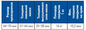
Таблица 2. Характеристики покрытия
Слой 31-32: tCream/bCream
Указанные слои содержат данные о нанесении паяльной пасты для пайки компонентов поверхностного монтажа. Как правило, этот слой используется изготовителями печатных плат в качестве шаблонов для нанесения паяльной пасты перед монтажом деталей.
При размещении компонентов поверхностного монтажа вся информация о том, куда следует наносить паяльную пасту, формируется автоматически. Однако если вам необходимо самостоятельно определить место нанесения паяльной пасты, обязательно сделайте область нанесения паяльной пасты меньше, чем область паяльной маски, чтобы два материала не перекрывали друг друга.
Проявление паяльной маски
Операция проявления паяльной маски при условии оптимального подбора режимов предварительной сушки и экспонирования проводится на стандартном оборудовании проявления, (аналогичным установкам, используемым для проявления травильного фоторезиста)
Однако при выполнении этой технологической операции надо обратить внимание на обеспечении тщательной отмывки (теплая вода, повышенная интенсивность струй), так как остатки неотмытого резиста паяльной маски после окончательного задубливания будут препятствовать нанесению паяемого покрытия на ламели печатных плат. Поэтому для проявления паяльной маски рекомендуется иметь отдельную установку
Solder Mask Considerations
Although, there is no clear consensus on why green is the predominant color used during the solder mask process, there are attributes that support its usage. First, green solder mask can be used to create the smallest solder mask dams (0.1 mm). Red, blue and yellow can produce dams of 0.12 mm. Black and white, which may provide the greatest contrast for your silkscreen, produce 0.15 mm solder mask dams. Supporting the usage of green may be the fact that green light has a wavelength of around 550 nm, which makes green the color most visible to the human eye in daylight.
However, color is but one of several considerations that influence the type of solder mask that must, or even can, be used. The primary consideration is the type of system in which the board will be deployed. PCBs destined for usage in certain industries or for certain applications must adhere to standards set forth in IPC-SM-840D.
To ensure that the solder mask process applied to your board meets all regulations, as well as your own requirements, you should partner with your contract manufacturer (CM) early in the design and development process. Engaging your CM will ensure that PCB assembly considerations, as well as the quality of your boards, will be well-integrated into the design and development process.
Tempo‘s Custom PCB Manufacturing Service
|
At Tempo Automation, we help you get started on the best path by furnishing information for your DFM and enable you to easily view and download DRC files. If you’re an Altium user, you can simply add these files to your PCB design software.
If you are ready to have your design manufactured, try our quote tool to upload your CAD and BOM files. If you want more information on the solder mask process and how it affects the manufacturing of your boards, contact us.
1 This is the board coverage or thickness of the solder mask based on the weight used.
Ограничения
- При создании тонкой перемычки (менее 75 мкм) она может повредиться в процессе монтажа и нарушить требуемую адгезию к поверхности ПП. Как результат – потеря свойств паяемости поврежденных контактных областей.
- Отсутствие возможности нанесения маски на концевые контакты разъемов/тестовые точки.
- При создании защитного слоя на печатных платах с выводным шагом более 1,25 мм, допускается попадание паяльной маски на контактные области только с одной стороны и не больше чем на 50 мкм. А при шаге менее 1,25 мм — не больше чем на 25 мкм.
- Все переходные отверстия, которые подлежат последующему покрытию защитной паяльной маски, должны быть закрыты (тентированы).
- Возможные дефекты: наличие областей с отсутствием защитной маски — менее 0,2 мм2 на 1 проводнике и меньше 2 мм2 на областях полигонов; наличие незначительных отслоений (до 0,25 мм); возникновение длинных туннельных пустот.
Surface finish
Regardless of the PCB solder mask types used, the resulting mask will leave behind certain exposed areas of copper on the circuit board. These exposed areas need to be plated with a suitable surface finish to prevent oxidation. One of the most popular surface finishes available is hot air solder leveling (HASL). Depending on the requirement other surface finishes also can be used such as electroless nickel electroless palladium immersion gold (ENEPIG) and electroless nickel immersion gold (ENIG). When needed, additional holes in the mask layer are left for the paste mask. This paste mask is utilized to attach pads or other components to the board based on the manufacturing process used.
To learn about black pad read, how to work around black pad in ENIG finish.
DOWNLOAD OUR DFM HANDBOOK:
Подготовка поверхности под сухого пленочного резиста и паяльную маску
Как уже говорилось, подготовки под сухой пленочный фоторезист (СПФ) и паяльную маску (ПМ) обеспечивают фотолитографическое формирование рисунка и поэтому очень схожи между собой. Они могут выполняться тремя способами (щеточной, гидроабразивной и химической обработкой) и в данной статье будут рассмотрены в одном разделе.
Во всех описаниях фоторезистов рекомендуемая шероховатость поверхности (Rz) достигает примерно 1–2 мкм. ГОСТ 53432–2009 «Платы печатные. Общие технические требования к производству» специфицирует необходимую шероховатость поверхности после ее подготовки как 1,5–2,5 мкм.
Слой 27-28: tValues/bValues
И вновь, согласно своим названиям, на этих двух слоях размещены номинальные значения каждого компонента на плате. Например, у резистора будет указано номинальное сопротивление, например 10К, а рядом с конденсатором можно увидеть значение емкости, например 0.1uF.
Многие разработчики решают не включать этот слой в физическую реализацию печатной платы, предпочитая вместо этого иметь спецификацию (Bill of Materials, BOM), к которой можно обратиться для того, чтобы уточнить номинальное значение по позиционному обозначению того или иного компонента. Однако если вы планируете разрабатывать печатную плату, которая будет частью набора для сборки, или которая будет собираться вручную, то будет чрезвычайно полезно представить на плате и позиционные обозначения, и номиналы компонентов. Это сделает процесс сборки более понятным.
Tips
-
Partial and complete tenting of pads and vias can be achieved by defining the appropriate value for the Expansion constraint:
- To partially tent a pad/via (covering the land area only) – if the expansion is from the land pattern perimeter, set the Expansion to a negative value that will close the mask right up to the pad/via hole. If the expansion is from the hole edge, simply set the Expansion to be 0.
- To completely tent a pad/via (covering the land and hole) – if the expansion is from the land pattern perimeter, set the Expansion to a negative value equal to, or greater than, the pad/via radius. If the expansion is from the hole edge, simply set the Expansion to be a negative value equal to, or greater than, the pad/via hole radius.
- To tent all pads/vias on a single layer, set the appropriate Expansion value and ensure that the scope of the rule (the Full Query) targets all pads/vias on the required layer.
- To completely tent all pads/vias in a design, in which varying pad/via sizes are defined, set the Expansion to a negative value equal to, or greater than, the largest pad/via radius.
- Solder mask expansion can be defined for pads and vias on an individual basis. While browsing properties for a pad or via through the Properties panel, options are available to follow the expansion defined in the applicable design rule, or to override the rule and apply a specified expansion directly to the individual pad or via in question. You can also force complete tenting of the pad/via on the top and/or bottom, using the Tented options in the Solder Mask Expansion section of the panel. When these options are disabled, the pad/via has no solder mask opening on the top/bottom of the board, and is therefore tented.
These options correspond to the Solder Mask Tenting — Top and Solder Mask Tenting — Bottom properties for the pad when viewing properties through the PCB List panel.
- Solder mask expansion can also be defined at the individual level for the following objects (through the Properties panel, when browsing the properties of a selected object): Track, Region, Fill, Arc. Options are available to follow the expansion defined in the applicable design rule, to override the rule and apply a specified expansion directly to the individual object in question, or to have no mask at all.
Solder mask processing with inkjet
PCB manufacturing has predominantly used inkjet systems to create nomenclature markings in the last decade. In recent years, however, technology has evolved enabling fabricators to print solder mask directly onto the board surface or panel surface. This is also sometimes called direct jetting (DJ), with the mask ink applied on the PCB surface according to the design input. The direct jetting is done through the use of a piezoelectric head.
Compared to the method based on photolithography, the DJ method cuts down most of the process steps leading to these advantages:
- Minimized material usage
- Reduced capital equipment and process variables
- Eco-friendly processing
- Elimination of excess use of solder mask
Applying solder mask onto a circuit board is a process that requires significant technical expertise and skill. To prevent board rejects and failure due to issues such as inadequate or excess reliefs, you need to select a PCB manufacturer who can handle this process without errors.
Want to learn more about solder mask layer? Let us know in the comments!
DOWNLOAD OUR IPC CLASS 3 DESIGN GUIDE:
Materials & Processes
When you discuss the materials and requirements for solder resist with your fabricator, you will have to take into account a number of factors:
- Class of application, T or H
- Physical size of the board
- Thickness of the conductors and the type of metallisation finish
- Track density on the surface, and how evenly spread the tracks are
- How many holes there are, of what size, and with what annular ring tolerance
- Whether components are placed on top of tracks
- Whether tented vias will be needed
- Whether the solder mask thickness will be important in defining the joint volume
The original solder mask was pattern-printed, using screen printing, but this technique has limitations on definition, with the result that photoimageable materials are used for most applications. As with any resist process, there is a choice between dry film materials, where a known thickness of mask is laid over the board, and liquid processes, where a deposit of approximately even thickness is attempted, typically in the case of solder resist by curtain coating.
You will appreciate from your study of Unit 2 that dry film materials adhere best to flat surfaces; given the necessarily uneven surface of the patterned board, a liquid photomask will be in more intimate contact with the foil and underlying laminate than a film type (Figure 1). For the highest definition, LPISM will generally be preferred, generally with a matte finish, because this reduces the potential of solder balling during reflow.
Figure 1: Example of dry film resist side walls
See our blog post titled Matte vs Gloss Solder Mask in Circuit Board Design for more information.
Прямое формирование рисунка паяльной маски струйным принтером
Операция прямого формирования рисунка печатных плат струйным принтером, в отличии от прямого экспонирования, позволяет обойтись без этапа фотолитографических операций.
Установки прямого формирования рисунка используют технику струйной печати. Их принцип действия основан на так называемой системе «капля- по-запросу» (DOD — drop-on-demand) c пьезоэлектрической генерацией капель. Принцип работы печатающих головок таких принтеров представлен на рис 129.
С помощью струйного принтера можно наносить различные материалы, используемые при изготовлении печатных плат
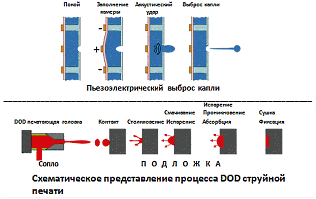
Рис. 129. Принцип работы пьезоэлектрическихи DOD печатающих головок
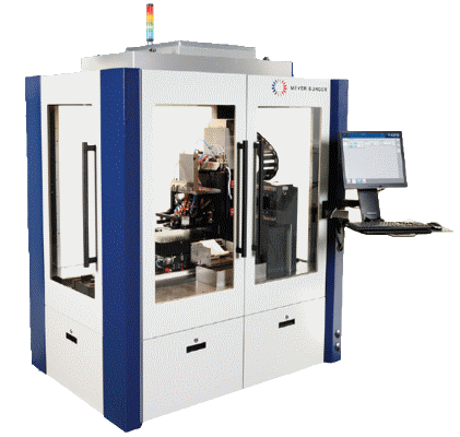
Рис. 130.Струйный принтер нанесенипаяльной маски фирмы MEYER BURGER
Помимо обычных графических приложений, струйную печать активно пытаются адаптировать для нанесения различных функциональных материалов, используемых в производстве печатных плат, тем более, что она позволяет создавать структуры с высоким разрешением.
Что касается паяльной маски — сокращение числа технологических операций при ее нанесении позволяет при использовании техники прямого формирования рисунка паяльной маски струйной печатью избавиться от большого количества технологических операций (и, соответственно оборудования, требуемого для их выполнения). Для реализации процесса потребуется только принтер и установка термодубления.
На Продуктронике 2017 в Мюнхене были представлены несколько установок струйной печати паяльной маски. Одна из которых ( разработанная фирмой MEYER BURGER) представлена на рис. 130. Известно, что существенным фактором, позволяющим использовать конкретную операцию в реальном производстве является доступность расходного материала.
MEYER BURGER активно сотрудничает с таким крупным производителем паяльной маски как Electra и Agfa, что вселяет уверенность в скорейшем комплексном освоении процесса и представлении принтера и паяльной маски, как единого коммерческого продукта. Кроме того фирма нашла интересное решение одной из сложных проблем процесса струйной печати именно паяльной маски. См. рис. 131.
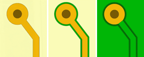
Рис. 131. Поэтапное формировыание рисунка паяльной маски на струйном принтере
Дело в том, что при нанесении паяльной маски необходимо покрыть до ≈90% площади заготовки (в отличие от 3-5% для маркировки. Где струйные принтеры давно и успешно применяются), что существенно увеличивает трудоемкость процесса.
Ф. MEYER BURGER разработала технологию нанесения паяльной маски прецизионными каплями по контуру рисунка с последующим заполнением контура крупными каплями , что значительно уменьшает трудоемкость и соответственно увеличивает производительность на данной операции.
В 2019 на форуме Issue EIPC опубликована информация о разработке на фирме состава Agfa DiPaMat SolderMask для струйной печати паяльной маски вносящей существенный вклад в разработку установки струйной печати PiXDRO для производства печатных плат (PCB) фирмы Meyer Burger. Использование установки струйной печати PiXDRO в сочетании с паяльной маской Agfa DiPaMat SolderMask заменяет традиционный субтрактивный метод , при котором сперва вся поверхность печатной платы покрыта сплошным слоем фотоформируемого состава , а затем выборочно удаляется с некоторых участков.
Установка PiXDRO от Meyer Burger предусматривает использование DiPaMat SolderMask, что позволяет компании представить полностью оптимизированное и готовое к продаже решение для струйного нанесения паяльной маски. DiPaMat SolderMask — УФ-краска для струйной печати, не содержащая растворителей. У нее лучше всего сбалансированы свойства вязкости и отверждения для обеспечения гибкой настройки и быстрой интеграции с большинством основных струйных печатных машин.
Фирма Agfa представила целую линейку составов под торговой маркой DiPaMat. Это торговая марка линейки материалов, пригодных для нанесения струйной печатью в индустрии печатных плат. В портфолио входят чернила Legend (для маркировки), чернила Etch Resist (для травильного резиста), а также недавно выпущенный SolderMask (паяльная маска), что ставит Agfa в авангард перехода индустрии на струйные решения для производства печатных плат.
Types of solder mask
Solder masks are of different types and the selection of them depends on the application for which it will be used. Given below are the various types:
Top and bottom side masks
These are typically used by engineers to identify openings in the green solder mask, already applied on the PCB. This particular layer of solder mask is added through epoxy or film methods. Next, the component pins are soldered to the board utilizing the openings that have been registered using the masks.
The traces on the top-side of the board are called top traces and the corresponding solder mask used is called a top-side mask. Identical to the top-side mask, the bottom mask is used for the bottom side of the board.
Epoxy liquid solder masks
The most cost-effective option among solder masks is epoxy. It is a polymer that is silkscreened on the PCB. Silkscreening refers to a printing technique that uses a woven mesh to support ink-blocking patterns. The mesh enables the open areas to be identified for the process of ink transfer. This step is then followed by thermal curing.
Liquid photoimageable (LPI) solder masks
LPI solder masks are actually a mix of two distinct liquids. These liquids are kept separately and mixed right before the application of the mask layer to enable longer shelf life. LPI is also one of the more cost-effective options among various other types.
LPI is employed for curtain coat, screen printing, and spray applications. This mask is a blend of various polymers and solvents. A thin coating can be formed using this mask that can stick to the target area surface. After using this mask, the PCB will generally not require any final surface finish that is currently available.
Unlike conventional epoxy inks, LPI is sensitive to UV light. The panel is required to be covered with the mask and after a short ‘tack cure cycle’, the PCB is exposed to UV light using a UV laser or photolithography process.
Before mask application, the panels are subjected to cleaning and are checked for any sign of oxidation. This is done using a chemical solution, aluminum oxide solution, or using suspended pumice to scrub the panels.
One of the most popular techniques used to expose the panel surface to UV light is through the use of film tools and contact printers. The top and bottom sheets of the film are printed using emulsion to block areas that need to be soldered. Production panels and film are then fixed in position, making use of tooling on the printer and exposed to a UV light source simultaneously.
One method utilizes direct imaging that makes use of a laser. This technique does not need tooling or film as the laser is controlled through the use of fiducial markers placed on the copper template of the panel.
LPI masks are available in various colors such as green, black, red, yellow, white, and blue.
Dry film photoimageable solder masks
The use of dry film photoimageable solder masks requires vacuum lamination. This dry film is subjected to exposure and then developed. Post-development, openings are identified to generate a pattern, after which the components are soldered to the copper pads. High-density wiring boards benefit most from dry film solder masks as it does not flood the through-holes.
Какие существуют способы улучшения прокрываемость торцов проводников?
Данному дефекту (рис. 7) подвержены главным образом проводники, расположенные параллельно ракелю при его движении, а также тонкие проводники, попавшие в момент нанесения под параллельно расположенную нить сетки. Обычно для улучшения качества прокрытия применяют следующие методы:
- изменение угла натяжения сетки (22,5°) по отношению к направляющим рамы;
- изменение угла положения заготовки по отношению к ракелю (рис. 8а);
- изменение угла расположения ракеля по отношению к печатной плате (рис. 86).
Дополнительно улучшить прокрываемость можно следующими способами: снижением давления ракеля и скорости его движения, а также применением более мягкого материала ракеля. Использование сетки с более крупной ячейкой и более вязкого материала маски тоже улучшает качество.
Рис. 7. Дефект непрокрытия торцов проводников, так называемых «пропусков» (IPC-A-600)
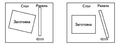
Рис. 8. Изменение угла расположения: а) заготовки к ракелю (слева); б) ракеля к заготовке (справа)
Manufacturing PCBs With Custom Colored
Applying a solder mask onto a circuit board is a tricky and demanding endeavor. Boards are known to fail due to solder mask issues like insufficient or extra-large mask reliefs or few or excess holes. Nevertheless, as the following DIY guide will show you, masking a PCB on your own is not impossible.
4.1 How To Solder Mask A PCB At Home
If you often make prototypes with old unmasked boards, knowing how to apply a solder mask can be a beneficial addition to your skillset. You can also save a significant amount of money by buying “naked” PCBs and doing the job yourself, depending on your board supplier and the size of your project.
Below is a list of the supplies you will need to mask a PCB.
- UV Curable Solder Mask Resin
- Transparent Film
- Nitrile gloves
- Isopropyl Alcohol
- X-Acto knife
- Ruler or T-square
- Cutting Mat
The essential items are the UV curable resin and the transparent film. UV curable resin hardens when exposed to ultra-violet light and is, therefore, a more sensible choice than thermal-cured mask materials.
The resin comes in different colors, and you can purchase it online or from a local electronics hobby store.
Making A Template
The first thing to do is to create a solder mask template using the transparent film. If your PCB design is simple, you can manually cut out the template by overlaying the film over the board and marking the pads and vias with a fine-tipped sharpie.
For more complex designs, use your CAD software to print your PCB layout onto the film. Designers commonly use inkjet printers with special “Quick-Dry” type transparency paper to draw out a template.
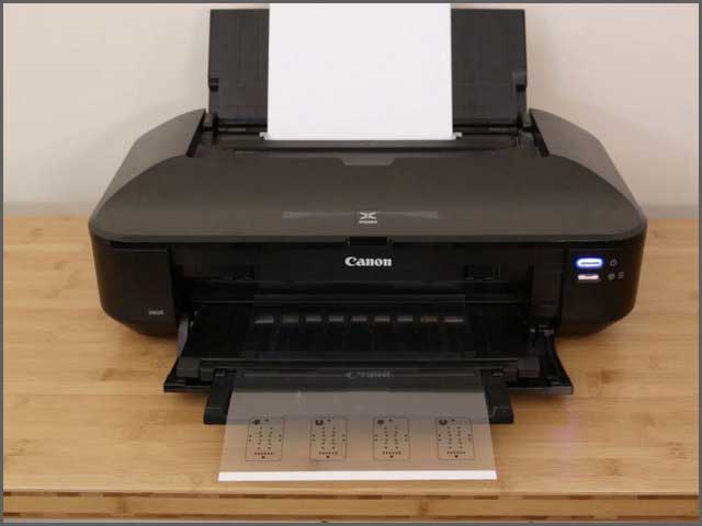
Figure 13: Printing a mask template with an inkjet printer(picture from adafruit)
Prepping The Film
Using your X-Acto knife, cut out the template from the paper, leaving some space around the edges for easy handling. You will need to add another printed template on top of your first one if the link doesn’t seem dark enough to block UV light.
Perfect alignment between the two sheets is crucial, so glue the edges together to stay in place.
Prepping The PCB
Before applying the resin, make sure your PCB is clean and rust-free. You can use a Scotch Brite pad to brush the board lightly and remove oxidation.
Applying The Resin
Place the clean board down on a new transparent film and use your fingers to press out the resin from the tube and onto the PCB surface. Use your best judgment to apply the amount of wax that will cover your entire board when you spread it.
Place another film on the PCB and squeeze down lightly to spread the resin. You can use your finger or a squeegee to make sure the wax reaches every corner and eliminate any air bubbles that may form.
Placing Your Template
When you’re satisfied with the resin application, set the film containing your template over the PCB and take your time to line it up correctly. You can add a drop of alcohol to the back of the template to adhere better to the film on the PCB.
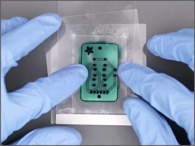
Figure 14: Perfect template alignment is key(picture from adafruit)
Exposing The Resin
Shine a consistently bright UV light source like an LED flashlight or lamp on the PCB. The light source you use should be large enough to cover the entire surface at once so that all board areas are exposed uniformly.
Peeling The Film
After exposure, carefully peel off the layers of film from the PCB. If you had exposed the resin enough, it would have hardened onto the board, and only the sections blocked by the ink on your template will be wet. You can then wash off the sticky resin to fully uncover the unmasked parts.
4.2 Factors To Consider When Masking A Board
As you have probably realized, masking a board demands a considerable deal of professionalism. To create a solder mask template for your PCB, you will need to take the utmost care to find the perfect alignment since a mistake can cause the mask to cover unintended areas.
You must also watch the sharpie or printer ink you use so that it’s dark enough to reflect UV light effectively, not to mention your type of light source, and how long to expose the resin so that it hardens sufficiently on the board.
Because of these overwhelming factors and the time required, most designers contact PCB manufacturers for their masking needs. Seeking professional help will be a better option for you than a DIY masking job, especially if you want a product that will stay functional for the long run.
If your project is sensitive and you wish to avoid costly mistakes, consider sending your files to a manufacturer and having the PCB made for you with the solder mask you want, rather than attempting to mask it yourself.
Щеточная обработка поверхности
Щеточная обработка (зачистка) выполняется абразивными валиками и является наиболее дешевой и производительной (рис. 1). Однако у данного метода есть недостаток: в ходе операции зачистки на поверхности формируются четко выраженные продольные риски в направлении движения заготовки (рис. 2).В случае если эти риски достигают глубины, которая при ламинировании не заполняется резистом за счет его пластической деформации, то при травлении они становятся источником растравов. Обычно это происходит в тех местах, где риски расположены поперек проводников (рис. 3).
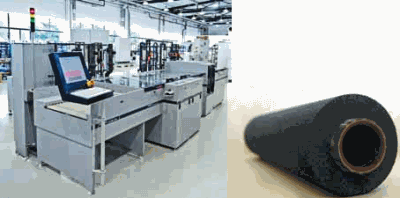
Рис. 1. Инструмент и оборудование щеточной зачистки
Рис. 2. Рельеф поверхности меди после щеточной зачистки
Рис. 3. Поверхностный растрав медных проводников в местах образования поперечных рисок после щеточной зачистки
Возможно, вам также будет интересно
Татьяна Смертина Все статьи цикла: Технология нанесения и обработки жидких защитных паяльных масок. Часть 1 Технология нанесения и обработки жидких защитных паяльных масок. Часть 2 Поводом для написания статьи стало возросшее количество вопросов, связанных с технологическими особенностями нанесения жидких паяльных масок. Наряду с тем, что многие крупные предприятия уже давно освоили технологию нанесения и успешно
Крепежные приспособления вибростенда нередко имеют резонансные частоты внутри диапазона испытаний, что может вызвать серьезные проблемы. Как правило, в этом случае испытатель пытается управлять шейкером с помощью акселерометра обратной связи, закрепленным на образце. Однако это позволяет лишь контролировать уровень вибрации в точке, где установлен акселерометр, и только. Повлиять на резонансы приспособления таким способом не удастся. Анализ
Force Measurement — новая опция SIPLACE для измерения усилия монтажа
15 ноября, 2012
Благодаря новой опции, разработанной специалистами SIPLACE, обладатели монтажных автоматов этой компании теперь способны предоставлять объективные доказательства качества своего производства.
Возможность контролировать правильность усилия SMT-монтажа компонентов является существенным преимуществом, особенно для производителей электроники, работающих с компонентами для поверхностного монтажа, чувствительных к давлению. Главным образом это касается отраслей, выпускающих автомобили и медицинское оборудование.
В прошлом доказать наличие отклонений усилий от заданных технических …
Summary
This rule checks the clearance between any silkscreen primitive and any solder mask primitive, or exposed copper-layer primitive (exposed through openings in the solder mask). The check ensures that the distance is equal to, or greater than, the value specified in the constraint.
Many manufacturers routinely strip (or ‘clip’) silkscreen to the mask opening and not just to the copper pad. However, doing so can render silkscreen text unreadable. Being able to catch such occurrences, through DRC, allows you to manipulate offending silkscreen text prior to sending the board to manufacturing.
All design rules are created and managed within the PCB Rules and Constraints Editor dialog. For a high-level view of working with the design rules system, see Constraining the Design — Design Rules. For detailed information regarding how to target the objects that you want a design rule to apply to, see Scoping Design Rules.
This design rule replaces the Silkscreen Over Component Pads rule found in previous releases of Altium Designer prior to Altium Designer 13.0. When loading a PCB document from such an earlier release, any defined Silkscreen Over Component Pads rules will automatically be converted to Silk To Solder Mask Clearance rules, with their scopes and constraints set to match legacy behavior. It is advised that you check your rule scopes and associated constraints to ensure accuracy in relation to design requirements.
Образование шариков припоя на паяльной маске
«Шарики припоя» — маленькие сферические вкрапления припоя на поверхности паяльной маски, приводящие к образованию перемычек (рис. 10). Раньше они удалялись на этапе отмывки, который обычно следовал за пайкой. В настоящее время отмывка применяется не так широко, как прежде, вследствие широкого распространения безотмывочных флюсов.
Появление шариков припоя особенно опасно на платах с тонкими проводниками, где наиболее вероятно образование перемычек.
Паяльные маски с глянцевой поверхностью более склонны к образованию шариков припоя, чем с матовой поверхностью. Существует несколько гипотез, объясняющих причины возникновения . 1. Одна гипотеза состоит в следующем: несмотря на тот факт, что в силу микрорельефа матовой паяльной маски площадь поверхности значительно увеличивается, площадь, к которой может прикрепиться шарик припоя, уменьшается. Шарики
припоя могут крепиться только к вершинам выступов (рис. 11).
2. Другая заключается в том, что матовая поверхность выступает в качестве резервуара, в котором задерживается флюс, который обеспечивает теплоотвод, предотвращающий повышение температуры поверхности паяльной маски выше температуры стеклования — точки, при которой маска размягчается и образует липкую поверхность, к которой и пристают шарики припоя.
3. Еще одно возможное объяснение состоит в том, что флюс, удерживаемый матовой поверхностью, испаряется при прохождении над волной припоя. Испаряющийся флюс сдувает с поверхности платы шарики припоя, отстающие от заднего края волны припоя.
Несмотря на множество гипотез, статистика практического опыта однозначна. Использование паяльных масок, образующих матовую поверхность, снижает количество образующихся шариков припоя.
Итак, мы рассмотрели технологические особенности процесса нанесения паяльной маски. В таблице 4 собраны общие рекомендации по возможным проблемам при нанесении паяльной маски и способам их устранения.
Решив вопросы технологии нанесения и обработки жидких паяльных масок, необходимо также особое внимание уделить подготовительным операциям: подготовке поверхности печатных плат перед нанесением маски и подготовке самого материала маски к работе
Слои 2-15: Route (Токопроводящие дорожки)
Возможно, данных слоев не будет в вашем ПО (Visible Layers dialog). В некоторых ПО они доступны только при премиум подписке. Слои 2-15 служат для формирования множества внутренних слоев для размещения токопроводящих дорожек в многослойных печатных платах. Для того чтобы воспользоваться ими, вам нужно будет изменить структуру слоев с помощью вкладки Tools » DRC » Layers. (в Autodesk Eagle).
Если вы планируете разработать многослойную печатную плату, то способы организации верхнего/нижнего и среднего слоя будет немного отличаться от того, что вы ожидаете увидеть. Например, при создании 4-слойной платы будут не просто использоваться слои 1, 2, 3 и 4 по порядку. Вероятнее всего, в системе разработке будут в комплексе использоваться слои 1 (верхний), 2, 15 и 16 (нижний).
How to Choose the Right Solder Mask Clearance for Your PCB
As with other tolerances for your PCB layout, your solder mask clearance should be tailored to your CM’s specifications. As we have seen, solder mask clearance is important to PCB assembly and, if inadequate, may lead to short circuits or even component destruction. Another important parameter that should be used as necessary to facilitate the PCB assembly process is solder mask expansion, which defines the separation between the solder mask and surface elements. In order to choose the right solder mask clearance for your PCB, you should consult your CM to ensure that your specifications fall within their equipment capabilities and requirements. It is also a good idea to consider the following:
| Additional Considerations for Choosing the Right Solder Mask Clearance for Your PCB | |
| Solder Mask Clearance Considerations | Why it is Important |
| Solder mask width | If it’s too narrow, the solder mask may pop off during PCB assembly. |
| Solder mask color | Different colors have different tolerance requirements. |
| Device sensitivity | Highly sensitive devices can be disrupted by leakage currents through the solder mask. |
By instituting these considerations as well as solar mask expansion into the DFM for your CM, you can optimize your usage of the space on your PCB.
Tempo‘s Custom PCB Manufacturing Service
|
Tempo Automation is the industry leader in fast turnkey PCB manufacturing for custom PCB design. Tempo employs an open and transparent “white box” approach to PCB manufacturing where the designer and CM form a symbiotic relationship to minimize the turnaround time and maximize the quality of your boards.
An essential aspect of this relationship is making our capabilities transparent and accessible; this includes solder mask specifications that will comprise the basis for your DFM. You can also easily view and download DRC files. If you’re an Altium user, you can simply add these files to your PCB design software.
If you are ready to have your design manufactured, try our quote tool to upload your CAD and BOM files. If you want more information on choosing the right solder mask clearance for your PCB or incorporating that choice into your design, contact us.
Похожие записи:
 Что такое прозвонка, и как проверить цепь на обрыв мультиметром
 Основные параметры конденсаторов
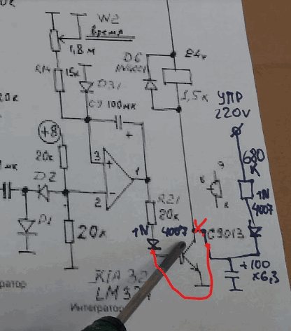 Как подключить и настроить датчик движения для управления освещением: электрические схемы подключения и настройка датчика
 Виды диэлектрических перчаток. перчатки диэлектрические: требования государственного стандарта
 Характеристики электронной лампы 6п3с
 Флюоресценция